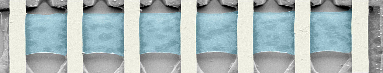
suspended CVD graphene

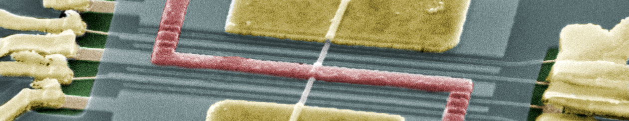

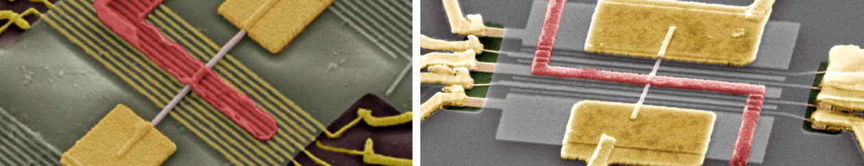
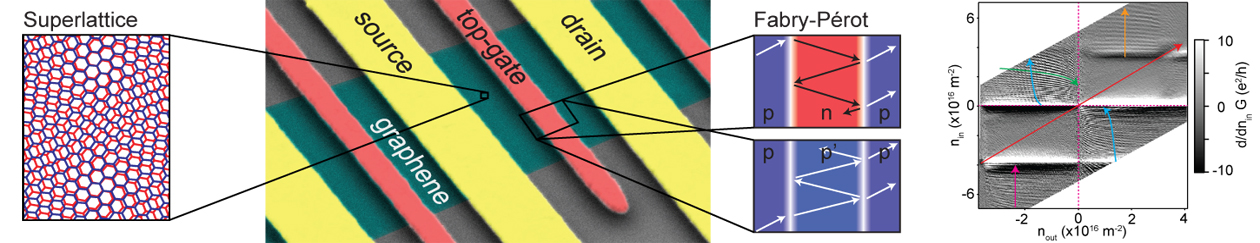
The nanoelectronics group is interested in fundamental electrical properties of engineered nanoscaled devices operating in the quantum regime. We probe these devices by electrical transport measurements both at low (close to DC) and high frequency (GHz range) and at cryogenic temperatures (Kelvin to milli Kelvin). Our devices are based on novel materials with reduced dimensions, either one-dimensional carbon-nanotubes (CNTs), quasi one-dimensional semiconducting nanowires (NWs) or two-dimensional graphene and van der Waals heterostructures which are defined by state-of-art e-beam lithography and complemented with gate and contact electrodes. The group is internationally recognized as a leader in so-called hybrid quantum devices that embody in addition to normal metal also superconducting and ferromagnetic electrodes. The latter introduce non-trivial correlations by proximity effect, such as a pairing or exchange field. In combination with intrinsic properties and surface effects, new correlated many-body states can arise. Examples are topological states such as the spin-helix states in one-dimension, molecular Andreev-bound states and Majorana-like states. In addition, we are working on suspended ultraclean devices that can additionally be driven mechanically allowing to explore the coupling between mechanical and electrical degrees of freedom at the quantum limit. Another strength of the group are short-noise measurements yielding information complementary to the conductance.
Research activities / projects: